Multi-layer Rogers PCB RO4350B Mixed Compression With FR4 Used In Aerospace Industry
Specification
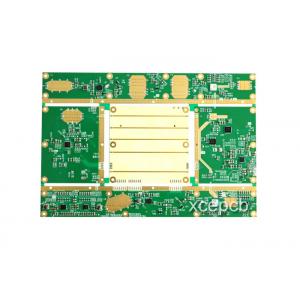
- 2 layer
- Green solder mask,
- white silk screen
- Model:XCER
- Size: 10*6cm
- Location: Shenzhen
Application:
a Telecom: transmitter. Receiver. Oscillator. Antenna.
b Satellite receiver
c Global location system, amplifier, satellite telecom
d Microwave transmission
e Automobile telephone
f Measure apparatus, LSI inspector, analyser, signal oscillator
g High frequency teletcom, high speed transmission, high security, high transmission quality, high
memory transaction
Parameter
| Board thickness tolerance | T≥0.8mm±8%,T<0.8mm±5% |
| Wall hole copper thickness | >0.025mm(1mil) |
| Finished hole | 0.2mm-6.3mm |
| Min line width | 4mil/4mil(0.1/0.1mm) |
| Min bonding pad space | 0.1mm(4mil) |
| PTH aperture tolerance | ±0.075mm(3mil) |
| NPTH aperture tolerance | ±0.05mm(2mil) |
| Hole site deviation | ±0.05mm(2mil) |
| Profile tolerance | ±0.10mm(4mil) |
| Board bend&warp | ≤0.7% |
| Insulation resistance | >1012Ωnormal |
| Through-hole resistance | <300Ωnormal |
| Electric strength | >1.3kv/mm |
| Current breakdown | 10A |
| Peel strength | 1.4N/mm |
| Soldmask regidity | >6H |
| Thermal stress | 288℃20Sec |
| Testing voltage | 50-300v |
| Min buried blind via | 0.2mm(8mil) |
| Outer cooper thickness | 1oz-5oz |
| Inner cooper thickness | 1/2 oz-4oz |
| Aspect ratio | 8:1 |
| SMT min green oil width | 0.08mm |
| Min green oil open window | 0.05mm |
| Insulation layer thickness | 0.075mm-5mm |
| Aperture | 0.2mm-0.6mm |
| Special technology | Inpedance,blind buried via,thick gold,aluminumPCB |
| Surface finish | HASL,lead free,Immersion gold,immersion tin,immersion silver,ENIG,Blue glue,gold plating |
Description:
The practical application of fast switching speed or high frequency PCB traces must be treated as transmission lines - its electronic properties to be controlled by the PCB design manufacturer of signal lines. That is, to a stable and predictable high-speed operation, the electronic properties of PCB traces and PCB insulating material must be controlled. One of the key parameters of PCB traces is its characteristic impedance. This is a relevant physical dimensions and PCB traces floor insulation material thickness function. Impedance of PCB trace inductance and capacitance reactance its decision.PCB transmission line typically consists of a wire traces, one or more reference layers and an insulating material composition. The dielectric constant of the transmission line ro4350b board that traces and sheet constitute a controlled impedance. PCB usually a multilayer structure, and controlled impedance can also be used to construct a multi-layer manner.