Add to Cart
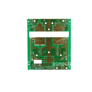
Fr4 High Speed Multilayer HDI PCB Board Fabrication With Impedance Control
Specification
PCB Type: | FR4 PCB |
Layer : | 4 layer |
Min .Line Width/Space: | 8milmil/8mil |
Min. Via Diameter: | 0.3mm |
Finish Thickness: | 20mil |
Surface Finish: | ENIG |
Size: | 3*6MM |
Material: | KB FR4 |
Color: | green |
Application: | aviation |
High frequency PCB Introduce:
| Model | Parameter | thickness(mm) | Permittivity(ER) |
| F4B | F4B | 0.38 | 2.2 |
| F4B | 0.55 | 2.23 | |
| F4B | 0.225,0.3,0.5,08,1,1.2,1.5,2,2.5,3.0 | 2.65 | |
| F4Bk | 0.8,1.5 | 2.65 | |
| F4B | 0.8 | 3.5 | |
| FE=F4BM | 1 | 2.2 | |
| Rogers | RO5880 | 0.254 0.508 0.762 | 2.20 ± 0.02 |
| RO4350 | 0.254 0.508,0.8,1.524 | 3.5 | |
| RO4003 | 0.508 | 3.38 | |
| TACONIC | TLF-35 | 0.8 | 3.5 |
| TLA-6 | 0.254,0.8,1,1.5, | 2.65 | |
| TLX-8 | 0.254,0.8,1,1.6 | 2.55 | |
| RF-60A | 0.64 | 6.15 | |
| TLY-5 | 0.254,0.508,0.8 | 2.2 | |
| TLC-32 | 0.8,1.5,3 | 3.2 | |
| TLA-35 | 0.8 | 3.2 | |
| ARLON | AD255C06099C | 1.5 | 2.55 |
| MCG0300CG | 0.8 | 3.7 | |
| AD0300C | 0.8 | 3 | |
| AD255C03099C | 0.8 | 2.55 | |
| AD255C04099C | 1 | 2.55 | |
| DLC220 | 1 | 2.2 |
Parameter
| Profile tolerance | ±0.10mm(4mil) | ||||||||
| Board bend&warp | ≤0.7% | ||||||||
| Insulation resistance | >1012Ωnormal | ||||||||
| Through-hole resistance | <300Ωnormal | ||||||||
| Electric strength | >1.3kv/mm | ||||||||
| Current breakdown | 10A | ||||||||
| Peel strength | 1.4N/mm | ||||||||
| Soldmask regidity | >6H | ||||||||
| Thermal stress | 288℃20Sec | ||||||||
| Testing voltage | 50-300v | ||||||||
| Min buried blind via | 0.2mm(8mil) | ||||||||
| Outer cooper thickness | 1oz-5oz | ||||||||
| Inner cooper thickness | 1/2 oz-4oz | ||||||||
| Aspect ratio | 8:1 | ||||||||
| SMT min green oil width | 0.08mm | ||||||||
| Min green oil open window | 0.05mm | ||||||||
| Insulation layer thickness | 0.075mm-5mm | ||||||||
| Aperture | 0.2mm-0.6mm | ||||||||
| Special technology | Inpedance,blind buried via,thick gold,aluminumPCB | ||||||||
| Surface finish | HASL,lead free,Immersion gold,immersion tin,immersion silver,ENIG,Blue glue,gold plating | ||||||||
Description:
FR4 Multi-Layer PCB refer to printed circuit board has more than two copper layers, such as 4L, 6L, 8L, 10L, 12L, etc. As technology improving, people can put more and more copper layers on the same board. Currently, we can produce 20L-32L FR4 PCB.
By this structure, engineer can put trace on different layers for different purpose, such as layers for power, for signal transfering, for EMI shielding, for components assembly, and so on. In order to avoid too many layers, Buried Via or Blind via will be designed in multi-layer PCB. For board more than 8 layers, high Tg FR4 material will be popular than normal Tg FR4.
More layers it is, more complex & difficult the manufacturing will be, and more expensive the cost will be. The lead time of multi-layer PCB is different from normal one, please contact us for accurate leading time.