F4BK350 High Frequency PCB High Speed Design Immersion Silver Surface GSM module 1.6MM
Specification:
High frequency pcb high-performance insulating material for microwave, radio frequency (RF) and high-speed digital signal processing (DSP) market with PTFE/type woven glass fiber fabric sheet.This material can be applied to LNAs LNBs, PCS/PCN antenna system, global positioning system (GPS) and UMTS antenna system,And the power amplifier, passive components, collision avoidance radar system, aviation help guide remote control technology and system of the phased array radar.
High frequency materials are UL 94V-0 rated for active devices and high power RF designs.
Specification:
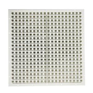
(1) F4BK350 mixed-compression PCB
(2) 2L high frequency pcb
(3) POS blind hole plate
(4) Professional PCB Manufacturer with 10 years' experience
Specification:
| Brand: XCE |
| Model: XCEH |
| Board size: 7*18cm |
| Cu thickness: 35UM |
| Material: F4B |
| Min line space&width: 4Mil |
Advantage
F4BK350 High Frequency PCB High Speed Design Immersion Silver Surface GSM module 1.6MM
1.Sufficient high frequency material raw
2. PCB Have the comprehensive quality control system
3. PCB good price
4. PCB quick turn delivery time from 48hours.
5. PCB certification(ISO/UL E354810/RoHS)
6. 12 years experience in exporting service
7. PCB is no MOQ/MOV.
8. PCB is high quality.Strict through theAOI(Automated Optical Inspection),QA/QC,fly porbe ,Etesting
Parameter:
| PRODUCT’S DETAILS |
| Raw Material |
F4B |
| Layer Count |
2-Layer |
| Board Thickness |
1.6mm |
| Copper Thickness |
35UM |
| Surface Finish |
Immerison Silver |
| Solder Mask |
/ |
| Silkscreen |
/ |
| Min. Trace Width/Spacing |
0.075/0.075mm |
| Min. Hole Size |
0.25mm |
| Hole Wall Copper Thickness |
≥20μm |
| Measurement |
60*159mm |
| Packaging |
Inner: Vacuum-packed in soft plastic bales
Outer: Cardboard Cartons with double straps |
| Application |
Communication,automobile,cell,computer,medical |
| Advantage |
Competitive Price,Fast Delivery,OEM&ODM,Free Samples, |
| Special Requirements |
Buried And Blind Via, Impedance Control, Via Plug,
BGA Soldering And Gold Finger Are Acceptable |
| Certification |
UL,ISO9001:2008,ROHS,REACH,SGS,HALOGEN-FREE |
Reference - our production capability for rigid PCB:
Layers: 1 to 28
Board finished thickness: 0.2 to 7.0mm
Materials: FR4,Rogers,Taconic
Max. finished board size: 23 x 25 (580 x 900mm)
Min. drilled hole size: 3mil (0.075mm)
Min. line width: 3mil (0.075mm)
Min. line spacing: 3mil (0.075mm)
Surface finish/treatment : HASL/HASL lead free,HAL, Chemicaltin, chemical gold
Immersion Silver/gold,OSP, gold plating
Copper thickness: 0.5-7.0oZ
Solder mask color: green/yellow/black/white/red/blue
Copper thickness in hole: >25.0μm (>1mil)
Inner packing: Vacuum packing/plastic bag
Outer packing: Standard carton packing
Shape tolerance: ±0.13
Hole tolerance: PTH: ±0.076 NPTH: ±0.05
Certificates: UL, ISO 9001, ISO 14001, SGS, RoHS
Special requirements: buried and blind Vias + controlled impedance + BGA
Profiling: Punching, routing, V-CUT, beveling
Provides OEM services to all sorts of printed circuit board assembly as well as electronic encased products
Parameter
| XCE PCB technical specifications |
| Material |
F4B |
| Layer No. |
2 |
| Min board thickness |
2 layer0.2mm
4 layer0.4mm
6 layer 0.6mm
8 layer 0.8mm
10 layer 1.0mm
|
| Max panel size |
508*610mm |
| Board thickness tolerance |
T≥0.8mm±8%.,T<0.8mm±5% |
| Wall hole copper thickness |
>0.025mm(1mil) |
| Finished hole |
0.2mm-6.3mm |
| Min line width |
4mil/4mil(0.1/0.1mm) |
| Min bonding pad space |
0.1mm(4mil) |
| PTH aperture tolerance |
±0.075mm(3mil) |
| NPTH aperture tolerance |
±0.05mm(2mil) |
| Hole site deviation |
±0.05mm(2mil) |
| Profile tolerance |
±0.10mm(4mil) |
| Board bend&warp |
≤0.7% |
| Insulation resistance |
>1012Ωnormal |
| Through-hole resistance |
<300Ωnormal |
| Electric strength |
>1.3kv/mm |
| Current breakdown |
10A |
| Peel strength |
1.4N/mm |
| Soldmask regidity |
>6H |
| Thermal stress |
288℃20Sec |
| Testing voltage |
50-300V |
| Min buried blind via |
0.2mm(8mil) |
| Outer copper thickness |
1oz-5oz |
| Inner cooper thickness |
1/2 oz-4oz |
| Aspect ratio |
8:1 |
| SMT min green oil width |
0.08mm |
| Min green oil open window |
0.05mm |
| Insulation layer thickless |
0.075mm-5mm |
| Taphole aperture |
0.2mm-0.6mm |
| Special technology |
Indepedance,Blind buried via,thick gold,aluminum PCB |
| Surface finish |
HASL,Lead free HASL,Immersion Gold, Immersion Tin,
Immersion Silver,OSP ,ENIG ,Golden finger,Blue glue,Gold plating
|