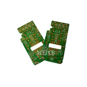
6 Layer Multilayer WIFI Printed Circuit Board For Audio Transmitter
Features:
>Glass-reinforced hydrocarbon and ceramic dielectric
>Excellent high frequency performance due to low dielectric tolerance and loss
>Stable electrical properties versus frequency
>Low Z-axis expansion and excellent dimensional stability
Specification:
| Base Material: Fr4 Material |
| Layer:6 |
| Thickness: 1.2MM |
| Copper weight:1OZ |
| Surface finish: HASL LF |
Since the day of company foundation we continuously enaged in researching special and high precision printed circuit boards with the strong production capability of 2 to 28 layers of highly precise impedence,multi-layer blind buried,multi-layer mix-compression,highTG, copper substrate,Ceramic substrate PCB.we emphasize the significance of traning program for every single staff in the company even grass-roots employees which becomes the most competitive factors to excel from others,our company have many experienced and professional teams from management to production line,30% are highly educated among the total amount of employees,advanced engineers and senior technicians are up to 80 people.
With advanced foreign technology supports and domestic 3G/4G device manufacturer in microwave pcb field which lead our experienced hi-frequencey researching team to one step ahead of the line of printed circuit board business,we are hornored to obtain sound reputations over our wolrdwide customers on the basis of fine qulity,prompt delivery,satisfied after sales service for may years and we assure our customers that we will return the favors with more and more superior products in the near future.
Applications:
High frequency high frequency wireless communication
High speed computer
Satellite signal transmission equipment
Microstrip and cellular base station
Antennas and power amplifiers
LNA/LNB
Parameter:
| Layer No. | 1-16 |
| Min board thickness | 2 layer 0.2mm |
| 4 layer 0.4mm |
| 6 layer 0.6mm |
| 8 layer 0.8mm |
| 10 layer 1.0mm |
| Max panel size | 508*610mm |
| Board thickness tolerance | T≥0.8mm±8%,T<0.8mm±5% |
| Wall hole copper thickness | >0.025mm(1mil) |
| Finished hole | 0.2mm-6.3mm |
| Min line width | 4mil/4mil(0.1/0.1mm) |
| Min bonding pad space | 0.1mm(4mil) |
| PTH aperture tolerance | ±0.075mm(3mil) |
| NPTH aperture tolerance | ±0.05mm(2mil) |
| Hole site deviation | ±0.05mm(2mil) |
| Profile tolerance | ±0.10mm(4mil) |
| Board bend&warp | ≤0.7% |
| Insulation resistance | >1012Ωnormal |
| Through-hole resistance | <300Ωnormal |
| Electric strength | >1.3kv/mm |
| Current breakdown | 10A |
| Peel strength | 1.4N/mm |
| Soldmask regidity | >6H |
| Thermal stress | 288℃20Sec |
| Testing voltage | 50-300v |
| Min buried blind via | 0.2mm(8mil) |
| Outer cooper thickness | 1oz-5oz |
| Inner cooper thickness | 1/2 oz-4oz |
| Aspect ratio | 8:1 |
| SMT min green oil width | 0.08mm |
| Min green oil open window | 0.05mm |
| Insulation layer thickness | 0.075mm-5mm |
| Aperture | 0.2mm-0.6mm |